Durostone Material Selective Wave Soldering for PCB Solder Pallets
Specification:
| Model | DurostoneCHP760 | DurostoneCAS761 | DurostoneCAG762 |
| Grade | Standard | Anti-Static | Anti-static(Optical) |
| Colour | Blue | Black | Grey |
| Density(g/mm3) | 1.85 | 1.85 | 1.85 |
| Standard OperationTemperature | 260 | 260 | 260 |
| Maximum Operation Temperature(C) | 350 | 350 | 350 |
| Sheet Size(mm) | 2440×1220 | 2440×1220 | 2440×1220 |
| Tickness/weight(mm/kg) | 3/17, 4/22 | 5/28, 6/33, 8/44 | 10/55, 12/66 |
Features and Benefits
Wave Soldering is a large-scale soldering process by which
electronic components (pin-through-hole components) are soldered to
a printed circuit board (PCB) to form an electronic assembly. CW's
wave pallets or solder pallets are designed to overcome the most
challenging situations. Each and every wave pallet or solder pallet
is custom designed to meet your needs. Tell us your challenges -
our experienced design staff has a proven solution for you.
Selective, Adjustable, and Rotating Fixtures, as well as Open
Apertures
Eliminate the need for expensive hand masking
Reduce costly defects and rejects
Accommodate multiple cards on same pallet
Improve throughput by quality and volume
Prevent warping
Allow standardization of conveyor width
Connector hold-down eliminates lifting or skewing
Wave pallets or solder pallets that work!
1 Eliminate flooding by masking open areas and preventing board
sag.
2 Reduce second hand load parts and hand soldering.
3 Save thousands of dollars in Kapton tape and the labor to add and
remove.
4 The composite materials thermally protect bottom side SMD’s from
shock.
5 Mask BGA vias from the wave ensuring reliable solder joints.
6 Lead Free grade optical material for higher temperatures
Used by most of our customers because of some advantages:
- Faster positioning on production line
- Low costs due to the missing of reinforced bars
- Better volume stocking
- Better yield with different board type on the production line
TOP SIDE STANDARD FEATURES
Chuangwei’s standard PCB hold down is our low profile. It is
unbreakable, ESD safe and guaranteed for the life of the pallet.
The non-marring design applies 12 pounds of downward pressure
without having to lift. Just twist! We also offer a high profile
hold down, cam-lock and custom hold downs for connectors.
Chuangwei does not ‘tap’ the composite, we use all “metal to metal”
fasteners ensuring a reliable and long lasting fixture.
We offer two sizes of extruded aluminum stiffeners and solder dams;
for smaller pallets we have a 3/8” tall and for larger pallets we
have a 3/4” tall design.
All pallets are engraved with the board name and our work order
number for handy reference. All data associated with your pallet is
stored to that work order number.
BOTTOM SIDE STANDARD FEATURES
All bottom side fasteners are made from 316 grade stainless steel.
This eliminates solder sticking or wetting to the fastener.
All fasteners are thread locked.
Our goal is to design and build a solution that will give you:
1. Highest yields with the largest process window possible.
2. Easy to use tooling that will survive your manufacturing
environment.
3. Fastest delivery times possible.
Process Suitability
The viability of this process route crucially relies upon being
able to estimate the number and distribution of PTH components
which CAN'T be processed (with and without glue dotting) - These
will have to be miniwaved or hand soldered.
which are likely to be poorly soldered - These will require further
inspection and manual touch up.
This estimation may be done in three ways
If a PCB is available (preferably populated) - our sales engineers
can rapidly evaluate your board.
If PCB design data is available we will process, analyse and
remotely assess it.
You can do it using the rules presented below - our customers
quickly find that the above two methods are easiest.
Gerber, Excellon and other data required
Pin Land to SMT pad clearance evaluation
The two figures below each show part of a CSWSC in plan and section
views. The right hand figure shows that more clearance
is required when the connector orientation is perpendicular to the
wave.
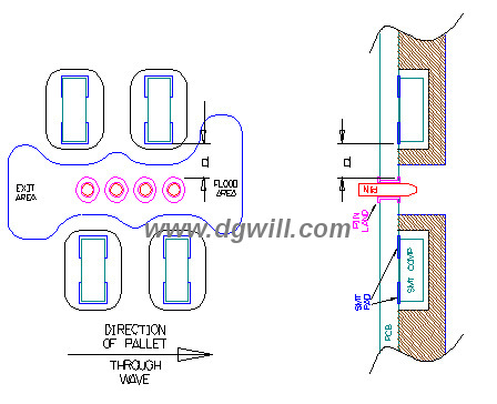
PTH Components Located Parallel to direction through wave
The clearance required between the pin land and SMT pad can be made
quite
small, as the solder does not have to flow "under" the component
pockets.
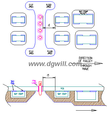
PTH Components Located Perpendicular to direction through wave.
A larger separation is required due to the solder having to flow
"under"
component pockets.
Working your way around the underside of the PCB, identify which
components
are parallel and perpendicular to the wave and assess the
solderability of each
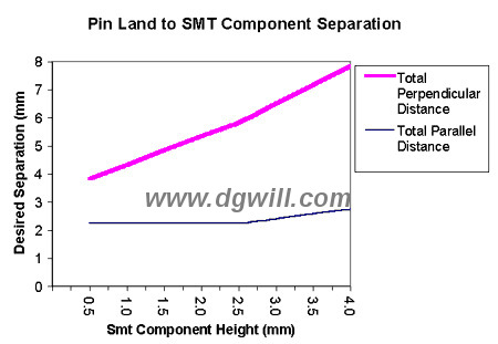
PTH connector by comparing the actual separation against the graph
right.
Ideally you want to be above the line in all cases.
PCB Design Implications - for Board Designers - or respin
We are often called upon by our customers to help with identifying
design respin opportunities.
We will identify problem areas within a board and suggest
appropriate movements of components. (Ideally before the PCB is
fabricated)
However for board designers reading this, can you remember another
four "rules" (to compete with the hundred other rules you have to
have floating
around in your head).
Keep large (height) SMT components away from PTH areas.
Leave the leading and trailing areas around PTH components as clear
as possible.
DON'T put any SMT components within 3mm (0.12") of any PTH
components.
DON'T put all PTH components in line along one edge of a board -
leave some space to allow us to support the masking in the centre
of the board.
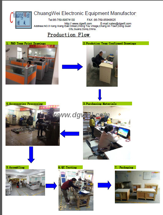
Our production flow
CE approval

Clients from electronic industry.


More information welcome to contact us:
Email/Skype: s5@smtfly.com
Mobile/Wechat/WhatsApp: +86-136-8490-4990


